Hierarchical schematic set
Organized, readable schematics with clear signal flow and logical partitioning by function.
Clear, hierarchical schematics in Altium Designer for analog, digital, RF, and high-speed circuits, verified by simulation before a single component is placed on a PCB.
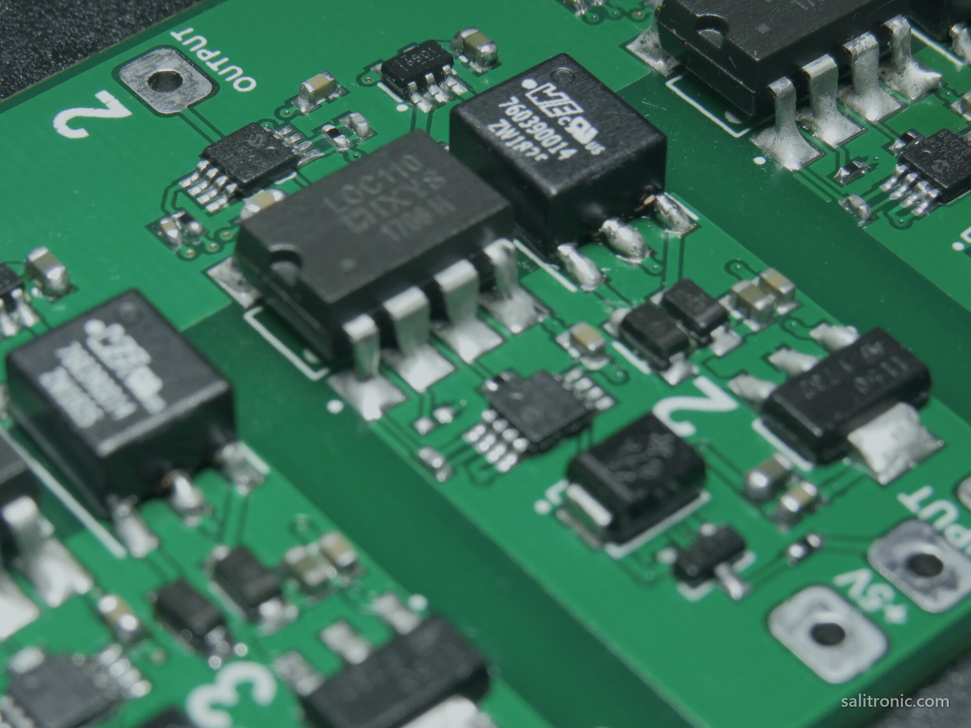
I design schematics across the full spectrum of electronic circuits: precision analog front-ends, high-speed digital interfaces, RF sections, power management, and mixed-signal designs. Each one is built with a hierarchical structure that keeps a complex design manageable and easy to review. Where it adds value, I run SPICE simulations on analog sections, signal integrity analysis on high-speed digital, and power distribution network analysis, so the design meets its specification before a single component is placed on a PCB. Whether the work stays in KiCad or Altium, clean schematic capture is where a design is really won or lost: correct parts, clear structure, and the review notes that stop an error propagating into layout.
Organized, readable schematics with clear signal flow and logical partitioning by function.
Verified component symbols with accurate pin mappings, linked to PCB footprints and supplier data.
A complete BOM with manufacturer part numbers, alternates, and supplier links.
SPICE simulation reports for critical analog circuits, including frequency response, transient analysis, and noise analysis.
Documented calculations for component values, power dissipation, timing, and other design parameters.
Annotated schematics highlighting critical areas, design decisions, and layout constraints.
Altium Designer project files for your records and future modifications.
Wrong voltage ratings, inadequate current capacity, or incompatible logic levels.
Lack of ESD protection, reverse polarity protection, or overcurrent limiting.
Insufficient decoupling, poor power sequencing, or inadequate bulk capacitance.
Impedance mismatches, crosstalk, or inadequate termination on high-speed signals.
Components operating outside safe temperature ranges under worst-case conditions.
Schematics that are difficult to read, review, or maintain.
I develop a block diagram showing the major functional blocks, interfaces, and signal flow, which establishes the hierarchical structure of the schematic.
I select components based on performance requirements, availability, cost, and reliability, and verify every part for current production status and lead times.
I design each functional block in detail, including component value calculations, simulation where needed, and application of best practices.
I create the formal schematics in Altium Designer with proper hierarchy, clear annotations, and design rule constraints for PCB layout.
I run a comprehensive design review including electrical rule check (ERC), simulation verification, and documentation review before proceeding to PCB layout.

An electronics design engineer with 20+ years of professional experience across analog, digital, RF, and power designs, delivered to clients in 15+ countries. Your project is handled by the person who has shipped hardware like it, start to finish.
See the project portfolioAltium Designer, with clean hierarchical schematics that are easy to review, maintain and hand off.
I do both. A schematic is most useful when the person drawing it is also thinking about the layout, so the two stay consistent.
Yes. I use simulation where it adds value to check critical parts of the circuit before committing to a board.
Yes. The deliverables are organised, readable schematics and a bill of materials that your team or a manufacturer can work from.
Yes. Schematic capture is done in KiCad or Altium, whichever your project uses, with correct component selection, a clear and reviewable structure, and a schematic review pass so mistakes are caught before they reach layout and become expensive.
Whether you need a complete schematic design or a review of an existing circuit, professional engineering makes sure your design works the first time.
Start the Conversation