PCB antenna design
Custom antenna geometries optimized for your PCB and enclosure, including inverted-F, meander, slot, and chip antenna integration.
Wireless connectivity engineered for the real world, from PCB antenna design and impedance matching to measured 3D radiation patterns, so your product works in the enclosure and not just in simulation.
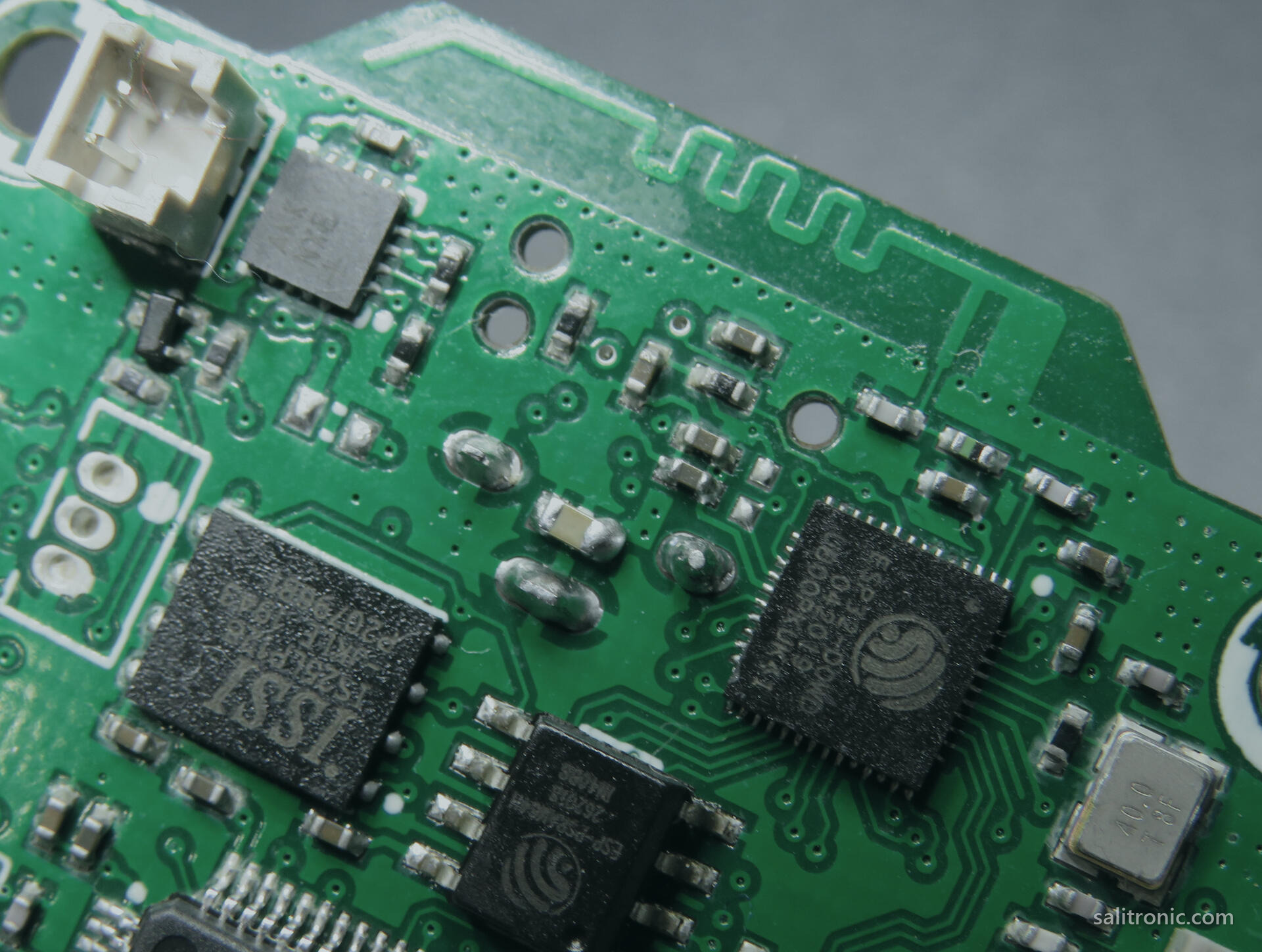
RF design is iterative by nature. Electromagnetic simulation gives a starting point, but real performance depends on enclosure materials, nearby components, and how the product is held and used. I fabricate prototypes quickly, measure impedance on my VNA, characterize the full 3D radiation pattern, and iterate until the antenna reaches maximum range while meeting your regulatory targets. This covers BLE product design on Nordic nRF52 and cellular IoT device design on the nRF91 for LTE-M and NB-IoT, from the antenna and matching through to the certification path. That includes BLE product design on Nordic nRF52 and nRF53, cellular IoT design on the nRF9160 and nRF9151 for LTE-M and NB-IoT, and the matching network and antenna tuning that decide whether either one actually reaches range.
A key strength is PCB-integrated antenna design. By designing antennas directly into the PCB, I reduce product cost while matching or improving on external antenna solutions.
Custom antenna geometries optimized for your PCB and enclosure, including inverted-F, meander, slot, and chip antenna integration.
Optimized impedance matching networks with component values verified by VNA measurement.
Full 3D radiation pattern measurements showing antenna gain and directivity.
Detailed guidelines for PCB layout including ground plane requirements, component placement, and trace routing.
Calculation of expected range under various conditions including path loss, antenna gains, and receiver sensitivity.
Recommendations for meeting FCC, CE, and other regulatory requirements for intentional radiators.
Documented measurements of return loss, efficiency, and radiation pattern.
High VSWR causing reduced range and wasted power dissipated as heat.
Antenna performance changing dramatically when placed in the final enclosure.
Insufficient or improperly shaped ground planes degrading antenna performance.
Digital noise coupling into RF sections and degrading receiver sensitivity.
Spurious emissions or excessive harmonics causing certification failures.
Products that work on the bench but fail to achieve expected range in deployment.
I define frequency bands, range requirements, antenna constraints, and regulatory targets, and evaluate enclosure materials and available PCB space.
I select the antenna topology based on your constraints. For PCB antennas, I develop the initial geometry through simulation, considering ground plane size and keep-out areas.
I fabricate prototype boards and measure antenna impedance with the VNA, tuning the matching network for optimal return loss at the target frequency.
I measure the full 3D radiation pattern to verify antenna gain, directivity, and polarization, and identify any pattern nulls or unexpected behavior.
I test performance in the final enclosure and iterate on the matching network if needed, then document the final performance specifications.

An electronics design engineer with 20+ years of professional experience across analog, digital, RF, and power designs, delivered to clients in 15+ countries. Your project is handled by the person who has shipped hardware like it, start to finish.
See the project portfolioSub-GHz and 2.4 GHz wireless, PCB and chip antennas, matching networks, and the RF front end of connected products. I handle layout, impedance control and the antenna tuning rather than just dropping in a module.
I measure. I tune matching on a VNA and check radiation patterns, so the antenna works in the real enclosure and not only in a simulation.
Yes. I review the existing RF section, find what is hurting efficiency or emissions, and revise the matching, layout or antenna to fix it.
Clients across Europe, the US, Canada, Australia and South Africa. The work is remote, with prototyping and RF measurement done in my lab.
Yes. BLE product design on Nordic nRF52 and similar Bluetooth Low Energy SoCs is a regular part of the work: antenna and matching, RF layout, coexistence, low-power firmware bring-up, and getting the radio through certification with real range.
Yes. Cellular IoT and nRF91 device design covers the LTE-M and NB-IoT front end, antenna and matching for the cellular bands, power and energy budgeting for battery operation, SIM or eSIM integration, and the path to carrier and regulatory approval.
Yes. Antenna choice, the matching network, and tuning against a VNA are part of the work, whether it is a chip or PCB antenna for a wearable BLE product on nRF52 or nRF53, or a cellular antenna for an nRF9160 or nRF9151 design on LTE-M and NB-IoT. Getting the match right is usually the difference between a link that holds and one that drops.
Yes. A GPS and GNSS tracker design combines the cellular link, often an nRF9160 or a SIM7600 modem, with a GNSS receiver, a power path sized for the duty cycle, and careful antenna isolation so the radios do not desensitise each other. The board is taken from schematic through layout to a tested prototype.
From Bluetooth to custom RF links, professional RF design ensures your wireless product achieves maximum range and passes certification.
Start the Conversation